- 您现在的位置:买卖IC网 > Sheet目录2001 > ISL5827INZ (Intersil)IC DAC DUAL 12BIT 3.3V 48-LQFP
7
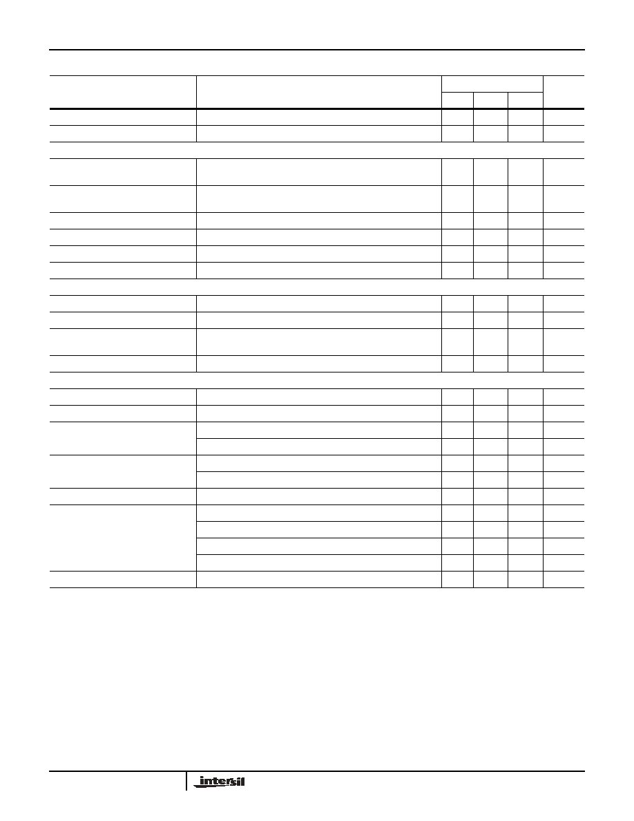
Reference Input Impedance
-1
-
M
Reference Input Multiplying Bandwidth (Note 8)
-
1.0
-
MHz
DIGITAL INPUTS D11-D0, CLK
Input Logic High Voltage with
3.3V Supply, VIH
(Note 3)
2.3
3.3
-
V
Input Logic Low Voltage with
3.3V Supply, VIL
(Note 3)
-
0
1.0
V
Sleep Input Current, IIH
-25
-
+25
A
Input Logic Current, IIH, IL
-20
-
+20
A
Clock Input Current, IIH, IL
-10
-
+10
A
Digital Input Capacitance, CIN
-3
-
pF
TIMING CHARACTERISTICS
Data Setup Time, tSU
See Figure 15
-
1.5
-
ns
Data Hold Time, tHLD
See Figure 15
-
1.5
-
ns
Propagation Delay Time, tPD
See Figure 15
-
1
-
Clock
Period
CLK Pulse Width, tPW1, tPW2
2
-
ns
POWER SUPPLY CHARACTERISTICS
AVDD Power Supply
(Note 9)
2.7
3.3
3.6
V
DVDD Power Supply
(Note 9)
2.7
3.3
3.6
V
Analog Supply Current (IAVDD)
3.3V, IOUTFS = 20mA
-
60
62
mA
3.3V, IOUTFS = 2mA
-
24
-
mA
Digital Supply Current (IDVDD)
3.3V (Note 5)
-
11
15
mA
3.3V (Note 6)
-
17
21
mA
Supply Current (IAVDD) Sleep Mode
3.3V, IOUTFS = Don’t Care
-
5
-
mA
Power Dissipation
3.3V, IOUTFS = 20mA (Note 5)
-
233
255
mW
3.3V, IOUTFS = 20mA (Note 6)
-
253
274
mW
3.3V, IOUTFS = 20mA (Note 7)
-
275
-
mW
3.3V, IOUTFS = 2mA (Note 5)
-
115
-
mW
Power Supply Rejection
Single Supply (Note 8)
-0.125
-
+0.125
%FSR/V
NOTES:
2. Gain Error measured as the error in the ratio between the full scale output current and the current through RSET (typically 625A). Ideally the
ratio should be 32.
3. Parameter guaranteed by design or characterization and not production tested.
4. Spectral measurements made with differential transformer coupled output and no external filtering. For multitone testing, the same pattern was
used at different clock rates, producing different output frequencies but at the same ratio to the clock rate.
5. Measured with the clock at 130MSPS and the output frequency at 10MHz.
6. Measured with the clock at 200MSPS and the output frequency at 20MHz.
7. Measured with the clock at 260MSPS and the output frequency at 40.4MHz.
8. See Definition of Specifications.
9. Recommended operation is from 3.0V to 3.6V. Operation below 3.0V is possible with some degradation in spectral performance. Reduction in
analog output current may be necessary to maintain spectral performance.
10. See Typical Performance plots.
Electrical Specifications
AVDD = DVDD = +3.3V, VREF = Internal 1.2V, IOUTFS = 20mA, TA = 25°C for All Typical Values (Continued)
PARAMETER
TEST CONDITIONS
TA = -40°C TO 85°C
UNITS
MIN
TYP
MAX
ISL5827
发布紧急采购,3分钟左右您将得到回复。
相关PDF资料
ISL5857IAZ
IC DAC 12-BIT 260MSPS 28-TSSOP
ISL5861/2IBZ
IC DAC 12BIT 210MSPS 28-SOIC
ISL5927INZ
IC DAC 14BIT CMOS DUAL 48LQFP
ISL5929INZ
IC DAC 14BIT CMOS DUAL 48LQFP
ISL5957IBZ
CONV D/A 14-BIT 3.3V 28-SOIC
ISL5961/2IBZ
CONV D/A 14-BIT 3.3V 28-SOIC
ISL59911IRZ
IC RCVR/EQUALZR TRPL DIFF 32QFN
ISL59913IRZ-T7
IC RCVR/EQUALZR TRPL DIFF 28-QFN
相关代理商/技术参数
ISL5829
制造商:INTERSIL 制造商全称:Intersil Corporation 功能描述:Dual 12-bit, +3.3V, 130/210MSPS, CommLink TM High Speed D/A Converter
ISL5829/2IN
功能描述:IC DAC DUAL 12BIT 3.3V 48-MQFP RoHS:否 类别:RF/IF 和 RFID >> RF 其它 IC 和模块 系列:- 标准包装:100 系列:*
ISL5829/2INZ
功能描述:IC DAC 12BIT CMOS DUAL 48LQFP RoHS:是 类别:RF/IF 和 RFID >> RF 其它 IC 和模块 系列:- 标准包装:100 系列:*
ISL58292IN
制造商:INTERSIL 制造商全称:Intersil Corporation 功能描述:Dual 12-bit, +3.3V, 130/210MSPS, CommLink TM High Speed D/A Converter
ISL5829EVAL1
功能描述:EVALUATION PLATFORM ISL5829 HS RoHS:否 类别:编程器,开发系统 >> 评估板 - 数模转换器 (DAC) 系列:CommLink™ 产品培训模块:Lead (SnPb) Finish for COTS
Obsolescence Mitigation Program 标准包装:1 系列:- DAC 的数量:4 位数:12 采样率(每秒):- 数据接口:串行,SPI? 设置时间:3µs DAC 型:电流/电压 工作温度:-40°C ~ 85°C 已供物品:板 已用 IC / 零件:MAX5581
ISL5829IN
功能描述:IC DAC DUAL 12BIT 3.3V 48-MQFP RoHS:否 类别:RF/IF 和 RFID >> RF 其它 IC 和模块 系列:- 标准包装:100 系列:*
ISL5829INZ
功能描述:IC CONV DUAL 12BIT 3.3V 48-LQFP RoHS:是 类别:RF/IF 和 RFID >> RF 其它 IC 和模块 系列:- 标准包装:100 系列:*
ISL58303DRTZ
功能描述:IC LASER DRVR 3CHAN 24TQFN RoHS:是 类别:集成电路 (IC) >> PMIC - 激光驱动器 系列:- 产品培训模块:Lead (SnPb) Finish for COTS
Obsolescence Mitigation Program 标准包装:60 系列:- 类型:激光二极管驱动器 数据速率:- 通道数:4 电源电压:3.3V 电流 - 电源:- 电流 - 调制:- 电流 - 偏置:- 工作温度:0°C ~ 70°C 封装/外壳:40-TQFN 裸露焊盘 供应商设备封装:40-TQFN EP 包装:托盘 安装类型:表面贴装